Submission 2025-04-24
Copying Data
1. Implement the function copy_asm_0 using only base instructions. The function should have the same functionality as its C counterpart.
File submissions/submission_25_04_24/copy_asm.s
2. Implement the function copy_asm_1 using only base instructions. The function should have the same functionality as its C counterpart.
File submissions/submission_25_04_24/copy_asm.s
Compile:
as copy_asm.s -o copy_asm.ogcc -c copy_c.c -o copy_c.og++ -o copy_driver.exe copy_driver.cpp copy_c.o copy_asm.o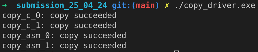
Instruction Throughput and Latency
- Files:
submissions/submission_25_05_24/ benchmark_driver.cppbenchmark.s
Compile: g++ benchmark_driver.cpp benchmark.s -o benchmark.exe
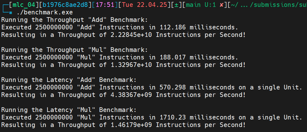
Output:
1. Microbenchmark the instruction throughput of ADD (shifted register) and MUL.
The first two blocks of the output shows the throughput benchmarks for ADD and MUL:
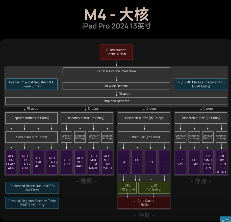
To better understand the throughput, we need to look at the architecture of a M4 performance core.
In the image below, we see that 8 ALU’s of different configurations are present.
As we use the ADD instruction only the ALU’s with the ADR specification are relevant to us, which are 5 out of 8.
Same goes for the MUL instruction, where we only have 3 out of 8 ALU’s able to perform multiplication.
With this knowledge we can now calculate the throughput of the ADD and MUL instruction.
ADD:
We have \(22.2845 \cdot 10^9\) instructions per second. That are \(22.2845 \cdot 10^9 / 5 = 4.4569 \cdot 10^9\) instructions per ALU per second. This aligns with a throughput of 1 instruction per cycle, as it is known from benchmarks that the performance cores of the M4 chip have a clock speed of 4.4 GHz.
MUL:
We have \(13.2967 \cdot 10^9\) instruction per second. That resolves to \(13.2967 \cdot 10^9 / 3 = 4.4322 \cdot 10^9\) instructions per ALU per second. This result also aligns with a throughput of 1 instruction per cycle for a known clock speed of 4.4 GHz.
2. Microbenchmark the instruction latency of ADD (shifted register) and MUL.
The last two blocks of the output shows the latency benchmarks for ADD and MUL.
Note, that we use read-after-write dependencies to measure the latency, thus we only use a single ALU for measurement.
ADD:
We have \(4.38367 \cdot 10^9\) instruction per seconds in a single ALU. Resulting in a latency of 1 cycle for the known clock speed of 4.4 GHz.
MUL:
We have \(1.46179 \cdot 10^9\) instruction per seconds in a single ALU. Resulting in a latency of \(4.4 \text{ GHz} / 1.46179 \cdot 10^9 \approx 3\) cycles.